Flip Chip Developments Open OEMs' Options in Miniaturized Assemblies

By Donald Styblo, Vice President of R&D, Valtronic USA Inc., and Philippe Clot, Vice President of Technology; Jean-Francois Zeberli, Sales & Marketing Technical Support; Jean-Marc Chenuz, R&D Engineer; and Frederic Ferrando, Process Engineer, Valtronic SA
Contents
C4 Process
Manufacturing Issues
Temperature Considerations
Summary
Manufacturers of miniaturized electronics face continuing pressure to meet conflicting goals. Complexity grows as synergistic functions are combined, but packages must shrink. Increased functionality places greater demands on designers to maintain usability. Failure mechanisms must be well understood and averted because repair is no longer feasible. Through it all, products must simultaneously support competitive pricing and return the high cost of design and development.
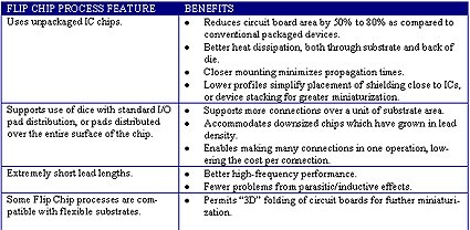
An answer to some of these challenges from an assembly standpoint is the "Flip Chip" process. Flip Chip was developed in the 1960s by IBM but is now attracting interest as a means of creating small, functionally dense electronic assemblies. Flip Chip sheds the unnecessary bulk of traditional integrated circuit packaging that can consume 50% to 80% of the surface area of a traditional electronic circuit. Flip Chip bonds unpackaged IC dice directly to circuit board substrates, without IC packaging or wire leads. Some of its benefits are summarized in Table 1.
Table 1. Flip Chip Benefits
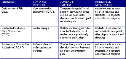
There are three general varieties of the Flip Chip process (Table 2) that differ chiefly in the electrical contact system and in the method used to attach dice to substrates. A common but important element in all three processes is the use of an "underfill" material between the die and substrate. Underfill is applied during or after the die bonding process to seal the die to the PC board, and to help counteract temperature-induced mechanical stress.
Table 2. Flip Chip Processes
C4 Process
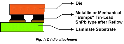
Controlled Collapse Chip Connection (C4) Flip Chip technology was developed by IBM in the 1960s as a method for attaching IC dice directly to circuit board substrates. As such, C4 has had a significant head start on other Flip Chip processes as a high-volume production tool, with estimates of a billion or more C4 connections being deployed in the field. The C4 process achieves attachment and electrical contact through the reflow of solder bumps previously applied to die pads (Fig. 1). The success of C4 is well documented, as are its limitations relating to larger chip sizes, higher contact densities, and temperature-related mechanical stress.
ACA Process
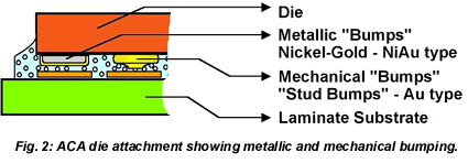
The Anisotropic Conductive Adhesive process (ACA) process uses an adhesive lightly loaded with metallic or metallized polymer particles, typically 3 µm to 5 µm in diameter, to simultaneously bond dice to substrates and make electrical contact (Fig. 2). The term "anisotropic" refers to the fact that particles in the adhesive are designed to make contact only between the chip and substrate (Z axis). The pressure applied during bonding squeezes particles away from each other, preventing contact along the X and Y axes. For reference, Isotropic Conductive Adhesives are more heavily loaded with conductive particles which make contact along the X, Y and Z axes. This property requires that ICA adhesives be locally applied to prevent shorts. ACA requires die pads to be metalized or bumped, and uses a moderate temperature (~200°C) to cure the adhesive.
Gold-on-Gold NCA Proces
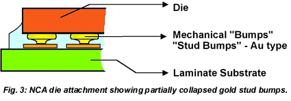
A variant of Flip Chip technology developed by Valtronic, Switzerland, uses a non-conductive adhesive to attach gold stud-bumped dice to laminate or polyimide flex circuit substrates (Fig. 3). This approach solves many of the limitations associated with other Flip Chip processes, including the ability to be used with ordinary dice or whole wafers, without any special preparation.
Manufacturing Issues
Flip Chip presents a number of challenges that can affect manufacturability, suitability-to-purpose, and long-term reliability. These relate directly to specific processes, and form the basis of the following discussion.
Die Pad Preparation and Contact Quality
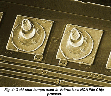
Most ICs are fabricated with aluminum contact pads which are neither directly solderable, nor compatible with conductive adhesives. For the C4 process, die pads can be prepared with additional metallization steps during wafer fabrication to provide a solderable surface. Similarly, the ACA process uses metallic bumping or coatings to provide a conductive surface for contact by adhesive particles. These steps are more difficult to accomplish with loose dice. The Valtronic process attaches gold stud bumps (Fig. 4) directly to standard aluminum die. Contact with copper-nickel-gold substrate pads yields a low-impedance contact having a typical resistance of less than 10 milliohms. This conductivity is comparable to solder, and considerably better than ACA's typical resistance of 25 to 50 milliohms.
It is possible to attach multiple dice using C4 processes, but all Flip Chip, surface mount, and through-hole components must be assembled in a single pass. With C4, reheating an existing assembly to attach additional components runs the risk of detaching previous solder joints. ACA and Gold-on-Gold Flip Chip enable dice to be attached individually, even at different times, without affecting previously bonded dice. Gold-on-Gold Flip Chip supports the finest contact pitch of the processes discussed here (100 µm to 150 µm). Its well-controlled stud-bump technology is unaffected by the possibility of short circuits from uncontrolled flow of solder or stray conductive particles, and it can be used for dice having 800 or more I/O connections arranged around the periphery or over the complete surface of a die.
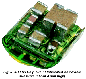
C4 results in the most rigid mechanical coupling between die and substrate, and thus, is most likely to be affected by mismatches in thermal coefficients of expansion (TCE). Organic substrates exhibit a higher TCE than silicon, making them less suitable for use with C4. Conversely, the use of an adhesive for die attachment makes ACA and Gold-on-Gold Flip Chip suitable to most substrate materials, including flex types. Flexible substrates facilitate 3D packaging where completed circuits are folded to form three-dimensional devices supporting the highest level of miniaturization (Fig. 5). Application of the adhesive to the clean substrate before chip placement results in the lowest possibility of underfill problems.
Temperature Considerations
Soldering has limited classical C4 Flip Chip to use with devices capable of withstanding 300°C to 350°C temperatures. A lower-temperature C4 variant (C4LT) uses temperatures around 270°C. However, these temperatures are still higher than the ~200°C temperatures typically required to cure adhesives. At temperatures of 400°C to 450°C, reactions can occur between IC pads and deposited metal films which result in chronic device failure, even though the product passes manufacturing tests.
Once a Flip Chip device has been placed in service, temperature-related factors can affect long-term reli-ability. Temperature cycling subjects the Flip Chip assembly to expansion and contraction. Solder-based processes rigidly couple the die to the substrate, which can result in the highest shear and axial stresses, especially with larger dice (Fig. 6). Organic and flex substrate materials are becoming more popular, but also exhibit the greatest TCE mismatch with silicon die materials.
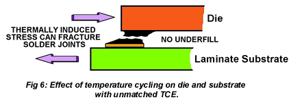
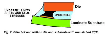
The reliability of solder-based Flip Chip processes has been improved by the application of an underfill, which reduces stresses placed on solder joints (Fig. 7). The effectiveness of the underfill requires thorough cleaning in order to avoid later problems such as underfill delamination and fracturing. With adhesive-based Flip Chip processes, the adhesive/underfill is applied to the clean, open substrate surface before the die is positioned, eliminating the possibility of voids. Thus, there is no need to rely on post-attachment cleaning or capillary action to spread underfill, as is necessary with C4.
A third concern with temperature is that long-term exposure to elevated temperatures, humidity, and harsh atmospheres can promote oxidation or corrosion of metals used in contacts, bumps, or conductive particles. Valtronic's contact system is based on noble metals, and has been tested with temperature cycling, elevated temperature storage, humidity, and salt fog tests without significant change in resistance (5 to 10 mW).
The ability to test a chip on the substrate before bonding can improve yield and help lower overall product costs. Solder-based Flip Chip processes are incompatible with testing during attachment because electrical contact is not achieved until the assembly is committed to the high-temperature soldering step. With adhesive-based processes, the die is forced against the substrate prior to curing of the adhesive, producing full electrical contact which facilitates testing before attachment. If testing indicates a problem, the die can be pulled from the board. Further, Gold-on-Gold Flip Chip is more tolerant than ACA of variations in flatness between substrate and die; stud bumps are typically four to eight times the height of conductive particles in a typical ACA adhesive.
Summary
C4 is the oldest Flip Chip process, and has proven to be commercially successful when used within the size and temperature constraints imposed by rigid, soldered die attachment. Some requirements, such as preparation of aluminum die pads, are more easily performed as a wafer fabrication step. Thus, C4 is geared more toward high-volume production. A sizable base of applications exists where C4 Flip Chip will remain the dominant method, even though its capabilities are gradually being overshadowed as dice migrate to-ward larger size, greater functional complexity, and denser contact spacing.
Anisotropic Conductive Adhesive (ACA) Flip Chip is suitable for more types of substrate material than C4, and provides better TCE performance. ACA relies on the compression of metallic or gold-coated polymer spheres suspended in the adhesive which is used to bond the die to the substrate. Aluminum die pads require preparation to assure contact, but contact resistance is generally higher than that of C4 or Gold-on-Gold Flip Chip. The ability to deal with close die contact spacing and multiple die attachment is better than C4, but is ultimately limited by the uniform distribution and behavior of these particles. Temperatures used to cure the adhesive are significantly lower than those needed for reflow soldering, reducing the possibility of semiconductor damage.
Valtronic's Gold-on-Gold Flip Chip process adds its own technological improvement to the most desirable attributes of C4 and ACA. The use of a gold stud bumps and substrate pads simplifies the function of the adhesive while achieving the same electrical high contact quality as soldered connections. Stud bumps also lend themselves to the use of ordinary dice, providing an economic advantage for small to medium production runs. The ability to accommodate multiple dice, close die spacing, and denser contact pitch surpasses the capabilities of C4 and ACA. Gold-on-Gold Flip Chip is compatible with a wide range of substrates, including flex types, and yields assemblies which are more resilient to stress resulting from temperature cycling and TCE mismatch. The use of low temperatures to cure the adhesive reduces the possibility of semiconductor damage.
As trends toward electronic miniaturization continue, Flip Chip will undoubtedly become more popular for achieving smaller sizes and higher performance impossible with conventional assembly techniques. Those considering Flip Chip should be aware that several varieties of Flip Chip exist, each with its own strengths. In many cases, newer versions of the process will enable manufacturers to get products to market faster and less expensively.
For more information, contact Donald Styblo, vice president of R&D, at 440-349-1239 (tel), 440-349-1040 (fax), or dstyblo@valtronic.com (email).
The Swiss contingent can be reached at +41-21-841-01-11 (tel), +41-21-841-02-22 (fax), or infoval@valtronic.ch (email).
Source: Electronic Engineering.com, sister website to Medical Design Online.
